Layer-by-layer thinning of two-dimensional materials
2024 / 04 庫碼教授(醫藥暨應用化學系)
Etching technology – one of the representative modern semiconductor device makers – serves as a broad descriptor for the process of removing material from the surfaces of various materials, whether partially or entirely. Meanwhile, thinning technology represents a novel and highly specialized approach within the realm of etching technology. It indicates the importance of achieving an exceptionally sophisticated and precise removal of material, layer-by-layer, at the nanoscale. Notably, thinning technology has gained substantial momentum, particularly in top–down strategies aimed at pushing the frontiers of nanoworlds. This rapid development in thinning technology has generated substantial interest among researchers from diverse backgrounds, including those in the fields of chemistry, physics, and engineering. Precisely and expertly controlling the layer numbers of 2D materials through the thinning procedure has been considered as a crucial step. This is because the thinning processes lead to variations in the electrical and optical characteristics.
In this comprehensive review, the strategies for top–down thinning of representative 2D materials (e.g., graphene, black phosphorus, MoS2, h-BN, WS2, MoSe2, and WSe2-based on conventional plasma-assisted thinning, integrated cyclic plasma-assisted thinning, laser-assisted thinning, metal-assisted splitting, and layer-resolved splitting are covered in detail, along with their mechanisms and benefits. Additionally, this review further explores the latest advancements in terms of the potential advantages of semiconductor devices achieved by top–down 2D material thinning procedures.
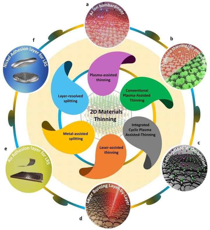
Fig. Modern layer-by-layer thinning technologies applicable to 2D materials utilizing: (a) plasma-assisted thinning, (b) conventional plasma-assisted thinning, (c) integrated cyclic plasma assisted-thinning, (d) laser-assisted thinning, (e) metal-assisted splitting, and (f) layer-resolved splitting.
出處:
Pham PV†, Mai TH†, Do HB, Vasundhara M, Nguyen VH, Nguyen T, Bui HV, Dao VD, Gupta RK, Ponnusamy VK*(庫碼), Park JH*. Layer-by-layer thinning of two-dimensional materials. Chem Soc Rev. 2024 Apr 8. doi: 10.1039/d3cs00817g.(SCIE, IF2023: 46.2, 2/178=1.12% in Chemistry, Multidisciplinary)
應用及亮點:
The thinning advances in processing materials have the potential to open up new opportunities for the development of high-quality 2D materials that are needed for electronics and optoelectronics for suitable applications including wearable devices, biomedical devices, e-vehicles and etc. The layer-by-layer thinning of 2D materials by integrated cyclic plasma thinning technology is regarded as the most promising method due to its minimal physical and chemical damage. By using thinning top–down approaches, it may be possible to fabricate ultra-thin, flexible, and transparent devices that efficiently harness and manipulate light at the nanoscale. This could open up new avenues for applications in wearable technology, displays, and advanced imaging systems. In addition, the thinning top–down strategies could also be beneficial in sectors like transportation. With the development of self-driving cars, the integration of numerous sensors, processors, and communication systems can lead to a highly complex and potentially unwieldy vehicle architecture.
